Chapter 7: Wafering Tab
The Wafering Tab in Yield-Pro is designed for creating and managing wafer slices from a crystal model. It offers several methods for wafer creation, including automatic and manual modes, and provides detailed options to fine-tune the wafering process for various crystal shapes and defect parameters.
Wafering Configuration
This sections allows user to configure the wafering process, including selecting the wafering method and defining some parameters.
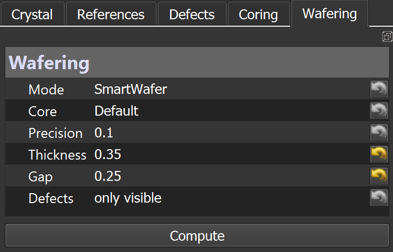
These are the possible parameters for wafering:
Core: Selects the core label to be used for wafering.
Offset: Adjusts the position of the wafer relative to the core.
Thickness: Sets the thickness of each wafer slice in millimeters.
Gap: Defines the gap between each wafer slice, allowing for precise control over the spacing.
Defects: Choose between only visible or all defects to determine which defects should be considered during wafer creation.
Precision (only for smart wafering): How much will the offset be adjusted to ensure the best possible yield during the smart wafering process. It refers to the accuracy and fineness of the cutting tool’s performance.
Axis: Defines the axis along which the wafering will occur, allowing precise control over slice orientation.
Wafer Mode
Creates regular cylindrical wafers, ideal for standard-shaped crystals with uniform geometry.
Smart Wafer Mode
Automatically adjusts the wafering to maximize usable material while avoiding defects. It takes into account both, the crystal shape and the defect distribution to optimize the process. More detail in Smart Wafering chapter.
Smart Wafer (Wire Saw) Mode
Beta version of the Smart Wafering mode, available soon in the upcoming version 4.8.17.
FreeZone Mode
Defines wafering zones based on minimum thickness and calculates the total amount of good material that can be obtained from the crystal. This option is best for crystals with irregular shapes or inconsistent material quality.
Slicing Mode
This feature enables the creation of slices in any shape or form, extending beyond cylindrical wafers. It is especially beneficial for uniquely shaped crystals where traditional cylindrical slicing methods are not feasible.
SlicingZone Mode
Similar to the FreeZone option, it is specifically tailored for crystals with irregular shapes. This mode establishes slicing zones by considering both the quality of the material and the shape of the crystal, with the goal of reducing waste.
Tip
By using options like Smart Wafering and Slicing Zone, you can optimize your yield and minimize waste, ensuring the most efficient use of your crystal material.
How to compute Wafers?
This gives you insight into how many usable wafers you can produce based on the settings you have configured. This step helps you visualize the impact of your choices and make adjustments to maximize yield.
To compute wafers, follow these steps:
Select the Wafering Mode: Choose the appropriate wafering mode based on your crystal shape and desired outcome.

Configure Parameters: Adjust the parameters such as core, offset, thickness, gap and so on.
Click on the
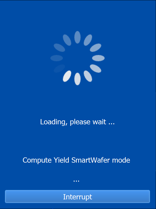
ComputeButton: This will initiate the wafering process, and a loading dialog will appear to indicate that the system is processing the wafers computation.
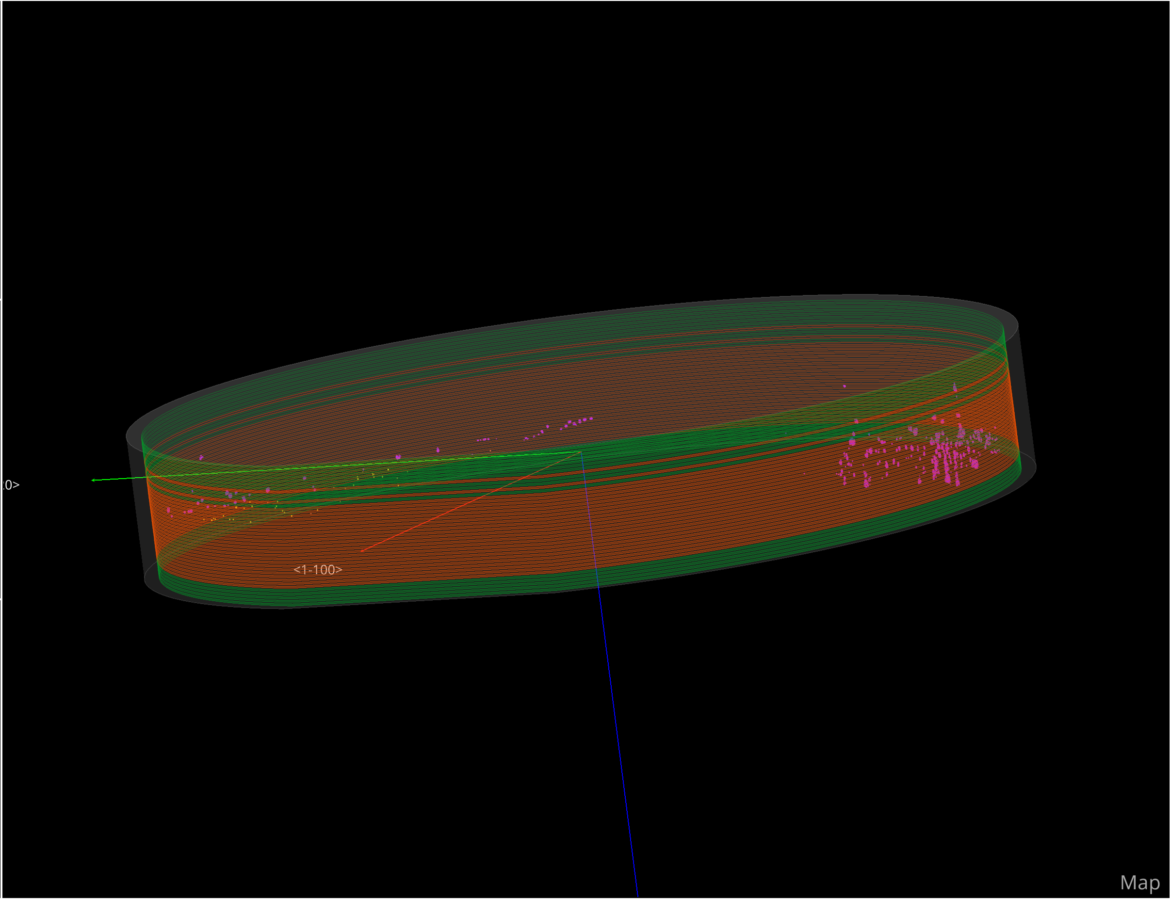
View Results: Once the computation is complete, you should have something similar to the picture below on your model:
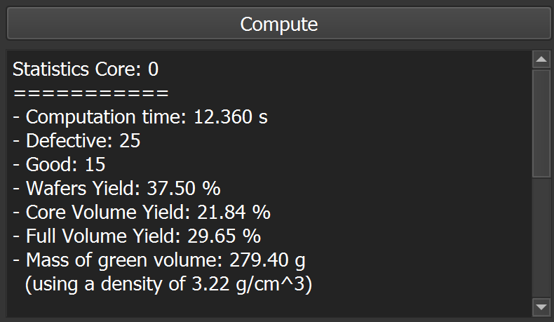
Statistics Section
After computing the wafers, the Statistics Section provides a detailed overview of the wafering results, including the number of defective and good wafers, as well as information for the cutting machine, will be displayed on the right-hand side under the Compute button. This data can be easily exported for further analysis or use during the cutting process.
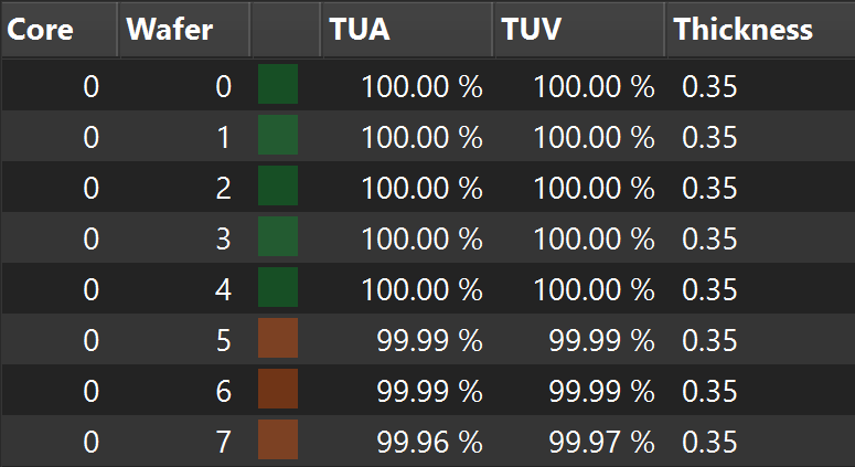
Wafer Details Section
The Wafer Details Section provides a list of all created wafers, with key information for each:
Core: The core number or label for reference.
Wafer: The specific wafer number in the sequence.
Color: The assigned color for the wafer in the visual model.
Top Usable Area (TUA): Amount of usable material at the top of the wafer.
Top Usable Volume (TUV): Volume of usable material at the top of the wafer.
Thickness: The thickness of each wafer.
This section lets you sort and review individual wafers to ensure they meet your production standards.
Tip
You can sort the wafers manually or click on the column headers to arrange them based on your preference and the chosen criterion.
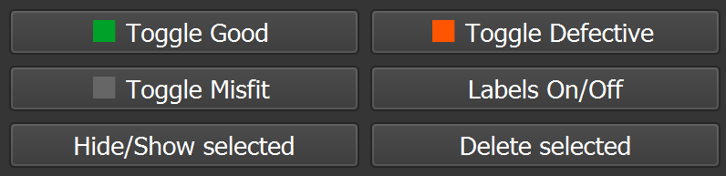
Action Buttons
Toggle Good: Highlights wafers that have a high yield of usable material.
Toggle Defective: Highlights wafers that are considered unusable due to defects or insufficient material.
Toggle Misfit: Highlights wafers that don't meet the specified criteria for usability but may still contain usable material.
Labels On/Off: Shows or hides the labels for each wafer, making it easier to identify them in the 3D view.
Hide/Show selected: Hides or displays the currently selected wafers in the main window.
Delete selected: Permanently deletes the selected wafers from the model. This action cannot be undone, so it should be used with caution.